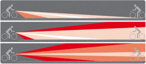
Many of our LED optical design projects start with a simple calculation. Basically, we tell a client how much mechanical space they need to reserve for a lens to achieve the beam angle or pattern they want. In all cases, the larger the LED chip, the bigger the optic and the smaller the beam angle, the bigger the optic. Sometimes this presents a problem.
A key detail in the calculation is ‘how big is the emission area of the chip?’ As it turns out, this is not always a simple question. The reason is that some LED’s have encased optics that sit on top of the phosphor magnifying the emission area.
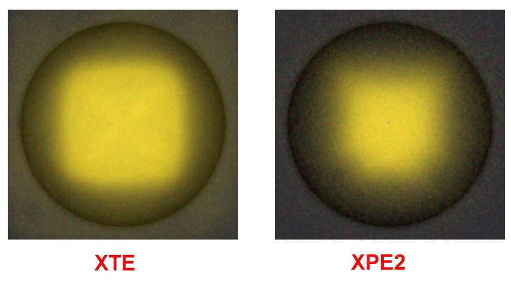
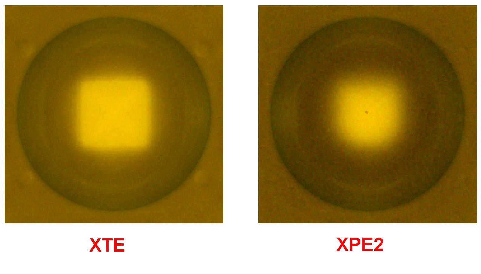
So every so often (it happened last week!) a client asks ” how big of an optic do we need to make our pattern with the CREE XTE or XPE2?”. We tell them “well, the XTE has about 2 x 2 mm, XPE2 has about 1.6 x 1.6mm emission area” after which the client hears from CREE “No! there is some mistake, OFH is confused XTE is a 1mm x 1mm.”
Why does this happen?
The two sets of images below show the XTE and XPE2 LED’s. The package size is the same but the left and right images have different phosphor sizes. Both of these LED’s have a lens on top and in the first image we see what the LED looks like in real life to a ray tracing program. The bottom image shows what the LED looks like if we ignore the lens on top.
What you will notice is in the top image, the emission area is larger than in the bottom image. For an optical engineers, the only data that matters is “where is the light when it hits my optic”. This is shown in the top image. While the bottom image shows light at the phosphor level is interesting, it is not helpful in determining how big a lens or reflector needs to be.
In effect neither CREE nor OFH is wrong: the phosphor is the size CREE says it is, but the LED emission area is functionally the size our engineers use.
Need help? Click here to learn more about our custom illumination optic design services.
Images may be used with permission. Data was prepared by Dr. Anatoli Trafimuk
