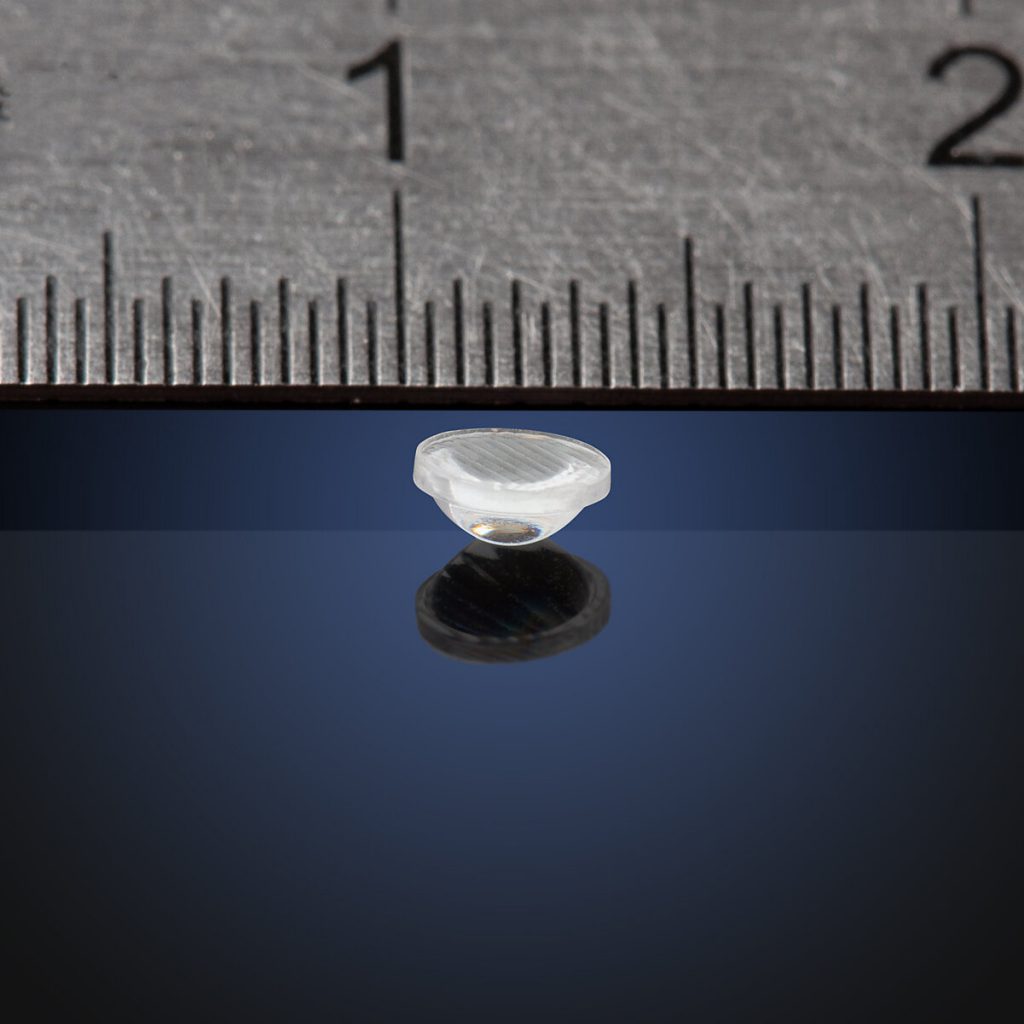
As optical systems are reduced in size, we encounter new engineering challenges when analyzing and designing lenses. These are issues that we usually don’t see when working with larger elements. This article will review some of the challenges when designing microlenses.
A microlens is roughly defined as a lens with a diameter lower than 1 mm to around 10 micrometers. Although their small size will reduce the presence of some type of aberrations, it will create some unexpected effects. For example, coma is usually minimized in microlenses, due to the fact that the aperture of the lens is itself small, but a microlens may introduce diffraction effects usually not observed on larger lenses. Similarly, due to the small aperture size of microlenses, they have an extremely large depth-of-field.
Fabrication Methods for Microlenses
An interesting consequence of working with microlenses is the limitation on fabrications techniques. In bulk optics, we can build lenses by grinding glass bulk to our desired shape, but with microlenses, this is more challenging. For high volume applications, this method is too expensive and time consuming; we instead require lithographic techniques, which limits the kind of materials that we use for our microlenses. Goodbye to BK, and LF types!
One very common method for microlens fabrication is called Thermal reflow Method. In this method, a photoresistor is deposited on a substrate and exposed to UV light through a mask. Once the photoresistor is exposed, we develop it leaving an array of cylinders. We then place the wafer in an oven where a flow of heat will melt the cylinders until they have a spherical profile.
Another method is by using molds. In this method, the polymer material is placed on a substrate and heated to almost melting point. Then a mold is applied by external pressure this deforming the polymer to the desired shape. Once the desired shape is achieved, the temperature is slowly decreased while the mold is removed.
There are additional methods that can be used to fabricate microlenses. One that I particularly like for its ingenuity, low cost, and high yield is the use of ink-jet technology. As in a regular ink-jet printer, a printer head deposits polymer drops on a substrate. These drops are then exposed to UV light solidifying the polymer to the desired shape.
Although microlenses are single optical elements, (there are very few micro doublet achromats reported in the scientific literature), we can design microlenses with different profiles: Spherical, Aspherical, Cylindrical, Freeform, and Fresnel.
Applications
Microlenses are an integral part of a wide variety of applications like Confocal Microscopes, Digital Projectors, LiDAR Systems, endoscopes, and many others.
Our Experience
At Optics For Hire, we developed microlenses for CARS (Coherent Anti-Stokes Raman Scattering) microscopy. CARS is a dye-free imaging technique to detect biological structures. One of the main advantages is that the samples are unaffected (as oppose to dye-based techniques).
In that system, we designed and fabricated the field lens, beam expander, and microscope lens. As shown in Figure 4, the CARS system involved more than one lens. Most of the optical components were fabricated using more traditional methods than the ones described in this paper. We cannot talk about specifics of the designs but we can say that the total length of the system is less than 5 cm and the smallest optical components have a diameter of less than 2 mm
Microlens Arrays
There are some applications where a single micro optical element is not enough. For example, CCD/CMOS sensors, usually required of microlenses in front of each photodetector. In those applications, we need to design microlens arrays. The fabrication techniques for microlens arrays are similar to single microlense ones with additional design parameters to consider.
Microlenses can be fabricated as a stand alone (usually when working as a coupler for optical guides) or as arrays. When designing a microlens array, it is necessary to define the configuration in which we will fabricate the lenses. Some common packing configurations are: square, hexagonal, circular, and random configurations.
Two additional design parameters for lenslet arrays are the pitch, which is the distance between to adjacent microlenses in the array (center-to-center), and the fill factor that is related to the distance between to adjacent microlenses (edge-to-edge). These parameters are of importance when designing microlenses for CMOS sensors with a high density of photodetectors.
Finally, we will mention that there are a wide variety of substrates that we can use. The choice of substrate depends not only on the polymer used for our microlens, but also on the application; whether we require a rigid or flexible substrate or not will limit our options. Regardless of the choice of substrate, we need to keep in mind its thickness and optical properties because they will affect the optical performance of our system.
Our Experience
We’ve often incorporated lenslet arrays for laser beam homogenization and beam shaping in TIR optics. In illumination design, it is common to design a single small angle TIR lens for a given LED and then add lenslet arrays to the exit aperture to widen the beam. This helps reduce mold tooling costs since the only new feature from, for example, a 15 degree beam angle TIR lens and a 30 degree, can be the lenslet array.

