Updated June 2020.
In our previous article, we discussed how to read optical drawings while in this installment, we will focus on surface finish details. Optical lens performance can be heavily affected by the lens surface roughness. The surface texture symbols are used in optical drawings to define a lens’s necessary surface finish and roughness and will the focus of this article.
Surface texture describes the surface waviness and roughness, lay, and flaw.
The surface finish symbols used in engineering drawings are defined by technical standards, such as ISO, ANSI, or AS (Australian standard). There are three surface roughness symbols (see figure below), indicating the surface (a), required material removal (b), and prohibiting material removal (c). The second one is most frequently used in optical engineering.

Surface finish symbols as defined by technical standards.
In the drawing below, we have shown three marks related to surface texture. Two identical marks for the front and back face, and one for side face.
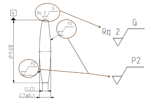
Surface texture Indicate by the three marks. Two identical marks for the front and back face, and one for the side face.
Need assistance designing a custom optic or imaging lens ? Learn more about our design services here.
The parameter is further described in various technical standards, including ISO standard. The full form of the said symbol is often not required, except in some applications where surface texture is crucial. An optical engineer running a ray-tracing program like Zemax will determine the allowable tolerances to achieve the desired performance. If these tolerances are not called out in production, drawing problems can occur, resulting in an unsuitable optical surface.
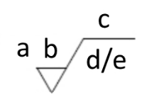
The ISO standard allows to define this parameter more precisely
Thus, full surface texture symbol will inform us of:
a is a type of roughness measurement – possible conventional signs are Rq (Root mean square (RMS) height variance) and PSD (Power spectral density (PSD) of surface height).
b is the value of Rq or PSD – unit of measurement is micrometer (µm).
c is the method and level of the surface treatment – possible conventional signs are G, P1, P2, P3, and P4. The ground method is used if a matte surface is needed, while P1, P2, P3, and P4 methods are used for polished surfaces. P level defines polishing quality. All the levels are described in the table.
| Level of the polishing | Number of the defects | Approximate roughness (in nm) |
| P1 | 80 < N < 400 | < 8 |
| P2 | 16 < N < 80 | < 4 |
| P3 | 3 < N < 16 | < 2 |
| P4 | N < 3 | < 1 |
- d\e parameter defines conditions for surface sampling – d is the value of minimum resolution for scanning of the profile surface. e is the value of the scan length. It is essential to note the units of measurement. As opposed to Rq and PSD values, which are measured in micrometer, these values are measured in millimeters (mm).
When ordering custom lenses, special care must be devoted to optical surfaces. As a rule of thumb, the higher quality surface roughness will improve product performance, but also make it harder to produce and more expensive. Thus, a best practice is to ensure you and your lens manufacturing vendor are using the same definitions related to lens quality.
